
chemical etching process for sem manufacturer Grasping strong production capability, advanced research strength and excellent service, Shanghai chemical etching process for sem supplier create the value and bring values to all of customers.
 WhatsApp)
A Novel Planarization Method Based on Photoinduced Confined Chemical ... confined chemical etching ... Cu surface and influence the etching process.
Wet Chemical Etching Process of BST Thin Films for Pyroelectric Infrared Detectors. ... Wet Chemical Etching Process of BST Thin Films for Pyroelectric Infrared ...
Etching Methodologies in 111 Oriented Silicon ... Abstract— New methodologies in anisotropic wetchemical etching of 111 oriented silicon, allowing useful process ...
This etching is a wetbased process that increases the ... (SEM) images of Si ... Nonlinear Etch Rate of AuAssisted Chemical Etching of Silicon ...
To solve the problems generally encountered during the plasma electrolytic oxidation (PEO) of Al alloys with high Si content, a pretreatment of chemical etching was ...
The Preparation of Silicon Nanowires Using MetalAssisted ... Silicon Nanowires Using MetalAssisted Chemical ... Chemical Etching, Silicon Nanowires, SEM.
To analyze the chemical etching process of InAs/GaSb ... SEM image of a cleaved mesa of the diode etched with the H 3PO 4/H 2O 2/H 2O solution at RT is shown in ...
Plasma Etching Outline ... Ideal Etching Process substrate film to be etched mask Before etch substrate ... Chemical Etching Ion Beam Methods Dry Etching
Chemical etching technique for porous and finegrain YBa2Cu307x superconductors with or without silver ... and finegrain YBa2Cu307x superconductors with or ...
Controllable fabrication of fiber nanotips by dynamic chemical etching based on siphon principle ... chemical etching process.
complementary chemical etching process, ... SEM images of an electrical discharge machined titanium microelectrode array that has undergone the chemical etching ...
The first of the two etching steps in the crystallographic etching process is used to ... SEM images of the two etch ... Crystallographic Wet Chemical Etching of p ...
channels and tunnels using femtosecond ... analysis of the etching process based on SEM ... and tunnels using femtosecond laser pulses and ...
fabricate AlN (Aluminum Nitride) piezoelectric microstructures for actuator applications. ... the AlN thin film during the sacial etching process ... (SEM). The ...
... dissolution of agarose stamp into hot water demonstrates an environmentally friendly method by the moldassisted chemical etching process ... SEM images of ...
... does not possess the ability to etch BST thin films annealed at high temperature, ... microscope (SEM) ... during the wet chemical etching process due to ...
chemical etching process. The chemical etchant used to ... Crosssectional SEM image of LEO GaN epilayer before etching process. (b–f) ...
Metalassisted chemical etching of CIGS thin films for grain ... wet chemical etching process to define CIGS ... can make the etching difference observable under SEM.
Dummy Poly Silicon Gate Removal by Wet Chemical Etching T ... for the dummy poly silicon gate removal process, ... that the TM wet chemical etching is a ...
This paper describes the optimized process of wetchemical etching of a ZnO ... the ZnO films to serve as the etching mask. The SEM photography of the etched sample ...
... and in particular to a process of crystallographic wet chemical etching of III ... field effect SEM image of ... etching process, ...
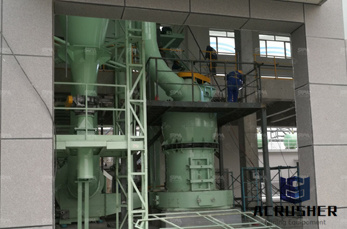
Home > Mining News > chemical etching process for sem. Information. Crushing Equipment; Grinding Equipment; Feeding Conveying; Screening Washing; Mobile .
Sputtering is a process whereby particles are ... and may be hard to distinguish from chemical etching. At elevated temperatures, chemical sputtering of carbon ...
Scanning Electron Microscopy (SEM) ... Cleaning problems and chemical etching ; ... Hazard investigation of exfoliants from manufacturing process;
WhatsApp)